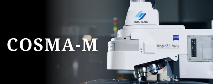
Benefiting from the rapid growth of artificial intelligence (AI), high-performance computing (HPC), and advanced packaging applications, the semiconductor industry continues to see increasing demand for high-precision metrology solutions. COSMA, a company with deep expertise in photomask inspection, recently announced the launch of the high-precision metrology system COSMA-M in collaboration with global optical technology leader ZEISS. Targeting the photomask, advanced packaging, and wafer metrology markets, the solution is designed to help customers enhance process control capabilities and improve manufacturing yields. This strategic partnership not only expands COSMA's product portfolio but also marks the company's official entry into wafer process metrology and advanced packaging inspection.
COSMA-M combines COSMA’s strengths in precision mechanical engineering and automation system integration with ZEISS’s advanced optical metrology technologies. The system delivers nanometer-level measurement accuracy, with measurement stability achieving a 3-sigma value of less than 3 nanometers, meeting the stringent requirements of advanced semiconductor processes. In addition, the equipment features a proprietary high-speed autofocus system and can be integrated with an EFEM (Equipment Front-End Module) for automated wafer loading and unloading, enabling a fully automated measurement workflow. This significantly improves production efficiency while ensuring measurement consistency and data reliability across manufacturing operations.
COSMA-M has already attracted strong interest from potential customers, with several companies submitting samples to COSMA for validation and testing. Current applications include DUV photomask critical dimension measurements, advanced packaging component inspection and metrology, TGV (Through-Glass Via) aperture measurements, as well as precision dimensional measurements for CPO (Co-Packaged Optics) components and Fiber Array Pitch.
Driven by the rapid growth of AI computing, CPO technology is gaining significant momentum, creating increasing demand for micron- and even nanometer-level measurement precision for photonic devices, silicon photonics chips, and optical modules. By entering the CPO metrology market, COSMA-M leverages its capability in critical dimension measurements, including Fiber Array Pitch, to support emerging silicon photonics and advanced optoelectronic packaging applications. This strategic expansion is expected to accelerate equipment adoption in high-volume manufacturing environments, enhance product value, and strengthen the company's presence in the high-end semiconductor metrology market.
COSMA stated that it will continue to deepen its technological collaboration with ZEISS while actively investing in the development of intelligent metrology, automated inspection, and AI-driven data analytics technologies. The company also plans to further expand its global market presence. As next-generation technologies such as advanced packaging, silicon photonics, and Co-Packaged Optics (CPO) enter a new phase of growth, COSMA is well positioned to benefit from the worldwide increase in semiconductor equipment investment. These trends are expected to create new momentum for future revenue and profitability, while supporting the company's long-term goal of becoming a leading domestic supplier of high-end semiconductor metrology equipment.